China Dragon Electronic Industrial Co., LTD Professional OEM PCB/PCBA Manufacturer Email:pcba@china-dragons.com
Language
China Dragon Electronic Industrial Co., LTD Professional OEM PCB/PCBA Manufacturer Email:pcba@china-dragons.com
China Dragon PCB processing process
1. Cutting
The copper clad plate raw materials, cut into the size we need, called opening.The process of cutting is to improve the utilization rate of raw materials and reduce the price of veneer.
11
2. Pretreatment
Remove the pollutants on the copper surface and increase the roughness of the copper surface to facilitate the subsequent film pressing process.
3. Lamination
The copper surface of the treated substrate is pasted with corrosion resistant dry film by hot pressing.
4. Exposure
The transfer of an image from the original film to a photographic substrate by the action of passing light.
5. Developing
The dry film without chemical reaction is washed away by lye action, and the dry film of reaction is left on the surface as a protective layer against etching.
6. Etching
The copper exposed after development is etched away with the use of liquid medicine to form the inner line graphics.The copper exposed after development is etched away with the use of liquid medicine to form the inner line graphics.
7. Remove the film
Strong alkali is used to peel off the corrosion resistant layer protecting the copper surface and expose the circuit pattern.
8. Punching
CCD is used to flush out the positioning hole and rivet hole.
9. AOI inspection
By automatic optical inspection, compare with sample or original data to find defects.
10. Drilling
A conductive hole is drilled on the PCB board surface for the line connection between layers.
11. Heavy copper
Remove burrs at the edges of holes to prevent poor plating.
12. Electroplating
Use electrolysis to prevent metal oxidation, and improve wear resistance and electrical conductivity.
13. Resistance welding
The parts that need to be welded on the PCB board are reserved, and other circuits and copper surfaces are covered to improve the electrical performance.
14. Screen printing
Convenient circuit maintenance and installation, logo and word code for annotation.
15. Surface treatment
PCB board surface treatment for better welding reliability, thermal stability, surface smoothness.
16. V - CUT
It is convenient and smooth to cut the original board into a single board process.
17. Test
Perform bare board test on electrical performance of PCB board to meet customer requirements.
18. Packing
Vacuum packing first, then safety packing
PCB Capacity
PCB fast samples
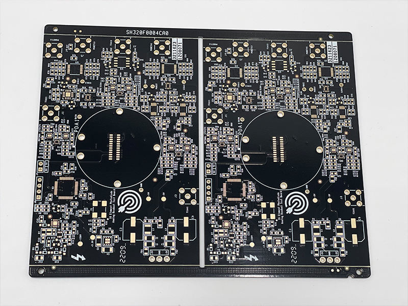
We are extremely good at providing customers with the shortest 24 hours of rapid circuit board proofing service.When your company needs fast circuit board proofing, you just need to send the documents to us, you can receive high quality circuit board in a very short time, and have a very attractive price competitiveness. In addition, we will also reflect the design problems found in your PCB sample making process in the trial production report.
All DFM manufacturability checks and process problem finding reports are free of charge. Many PCB rapid proofing companies in the market put more than a dozen boards together for material opening production, which will lead to many quality risks. However, we only produce proofing for each type of PCB separately to ensure quality and reduce the accuracy of PCB circuit simulation verification.
PCB multilayer board and complex process
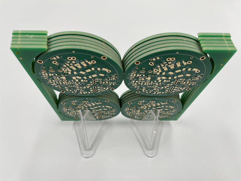
Support 1 to 48 layers of multi-layer plate, HDI, blind hole, BGA, disc hole, gold finger, resin plug hole, laser drilling, 3mIL line width line spacing and other complex processes.
Prototyping PCB Technologies
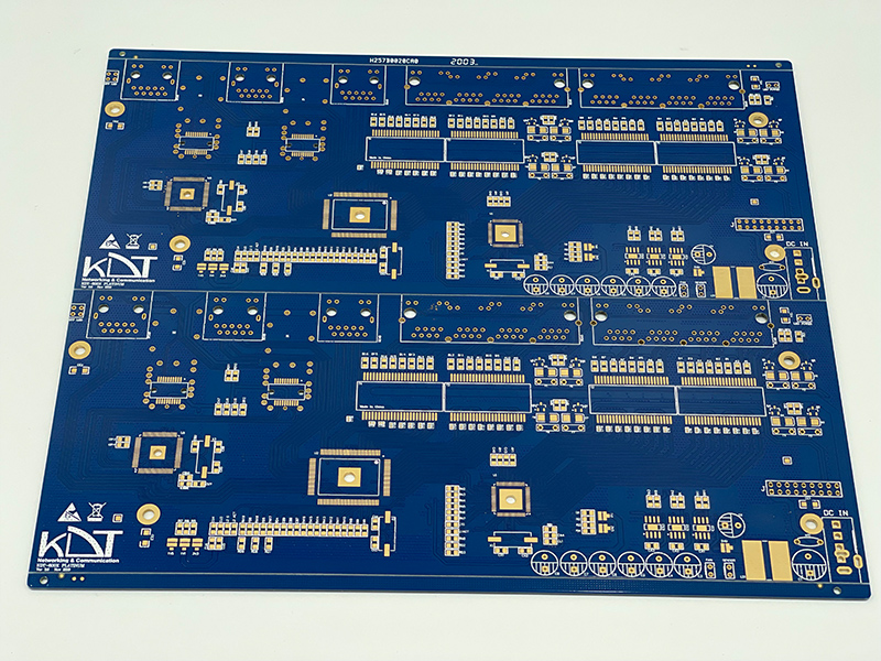
We can offer nearly limitless capabilities for our prototyping PCB services.
Whether our customers need single or double-sided FR4 pcb boards or very high technology blind and buried via boards, boards made with unique materials, China Dragon will be able to bridge your design concept with reality.
Our capabilities span a number of advanced technologies including thermal PCBs, microwave PCBs, heavy copper, rigid-flex PCBs, flex PCBs and MCPCB.
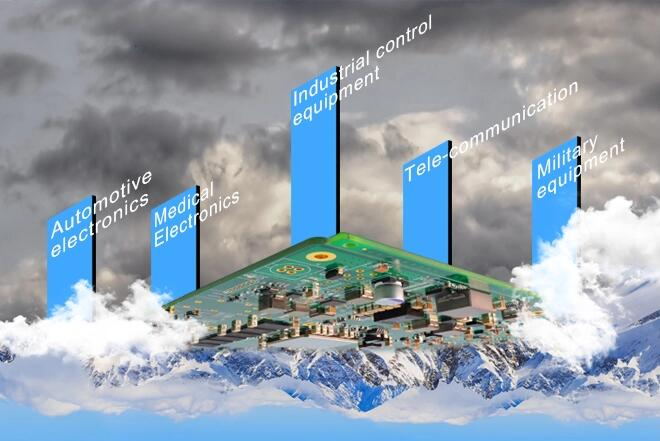
We have the capabilities to supply prototype boards for advanced industries and critical system designs, including:
* Aerospace
* Automotive
* High Performance Computing (HPC)
* Industrial
* Medical
* Military / Defense
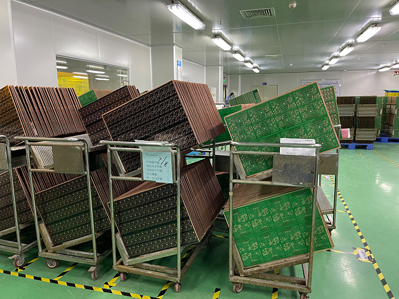
Advanced IPC standards are also adhered to, depending on technology
Our engineering staff is available to consult you throughout the layout, build, and testing phases of prototype manufacturing, moving your application through additional prototyping stages or into production.
When you have finalized your design and the application of your prototype PCBs, we are also capable of a full production run for your product/application, including full turnkey assembly, with tighter PCB tolerances.
Moving a prototype into production with us will also give you the benefit of no additional tooling fees.
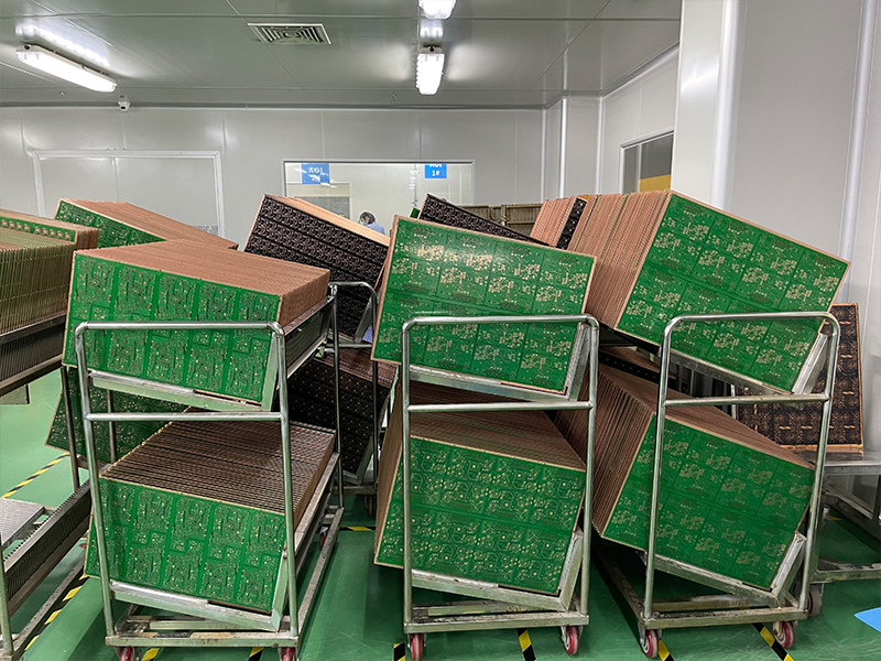
Testing Protocol
All of our prototype PCBs include standard fabrication tests and inspections:
* DFM testing & analysis
* Design & BOM validation
* Standard electrical validation test (EVT) via flying probe
A visual inspection is performed for PCB assembly.
Additional advanced testing can be requested, but will affect turnaround lead times.
View our entire PCB testing capabilities.
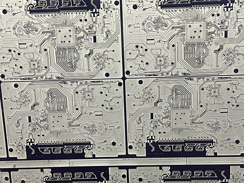
These standard tests will detect and assist with diagnosing many common issues, including:
* Design Flaws* Schematic Problems
* Circuitry Issues
* Component Shortages
PCB Prototypes vs. Production Capabilities
| Specifications | PCB Prototype Capabilities | Standard / Production PCB |
| Around | ||
| Number of Layers | 1 - 16 layers | Up to 48 layers |
| Min. Order Quantity | 1 Panel | N / A |
| Turn Around Time | 24 hours up to 6 Layers | 3 to 21 Days |
| 3 - 7 days for 6-16 Layers | ||
| Board Materials | Rigid PCB Materials | Rigid PCB Materials |
| FR4 | FR4 | |
| FR406 | FR406 | |
| 370HR | 370HR | |
| VT-47 | VT-47 | |
| FR408 | FR408 | |
| Arlon | Arlon | |
| CEM | CEM | |
| Megtron 6 | Megtron 6 | |
| Astra MT77 | Astra MT77 | |
| Tachyon 100G | Tachyon 100G | |
| Nelco 4000 | Nelco 4000 | |
| Rogers 3000 Series | Rogers 3000 Series | |
| Rogers 4000 Series | Rogers 4000 Series | |
| Rogers 5000 Series | Rogers 5000 Series | |
| Rogers 6000 Series | Rogers 6000 Series | |
| Taconic TLY | Taconic TLY | |
| Polyimide | Polyimide | |
| MCPCB, Aluminum Core & Copper Core Materials | MCPCB, Aluminum Core & Copper Core Materials | |
| Aluminum Core | Aluminum Core | |
| Copper Core | Copper Core | |
| Ventec VT-4A1/VT-4A2 | Ventec VT-4A1/VT-4A2 | |
| Aismalibar Fastherm | Aismalibar Fastherm | |
| Aismalibar Flextherm | Aismalibar Flextherm | |
| Flex PCB Materials | Flex PCB Materials | |
| Kapton | Kapton | |
| Shin-Etsu - Epoxy | Shin-Etsu - Epoxy | |
| Adhesive System | Adhesive System | |
| Rogers - Epoxy | Rogers - Epoxy | |
| Adhesive System | Adhesive System | |
| Dupont FR - FR Acrylic | Dupont FR - FR Acrylic | |
| Adhesive System | Adhesive System | |
| Dupont LF - LF Acrylic | Dupont LF - LF Acrylic | |
| Adhesive System | Adhesive System | |
| Adhesiveless Base Materials | Adhesiveless Base Materials | |
| Board Sizes | 16" x 22" | 16" x 22" |
| 12" x 21" | 12" x 21" | |
| 22" x 28" | 22" x 28" | |
| 10" x 16" | 10" x 16" | |
| 16" x 22" | 16" x 22" | |
| 12" x 21" | 12" x 21" | |
| Board Thickness | 2 layer - 0.010" | 2 layer - 0.010" |
| 4 layer - 0.020" | 4 layer - 0.020" | |
| 6 layer - 0.020" | 6 layer - 0.020" | |
| 8 layer - 0.062" | 8 layer - 0.062" | |
| 10 layer - 0.062" | 10 layer - 0.062" | |
| 12 layer - 0.062" | 12 layer - 0.062" | |
| 2 layer - 0.005" | 2 layer - 0.005" | |
| 4 layer - 0.010" | 4 layer - 0.010" | |
| 6 layer - 0.031" | 6 layer - 0.031" | |
| 8 layer - 0.040" | 8 layer - 0.040" | |
| Copper Thickness | 0.5 oz - 3 oz | 4 oz - 10 oz |
| Hole Aspect Ratio | 7:01 | 15:01 |
| Minimum Hole Size | 0.008" | |
| Minimum Trace/Space | 0.006"/0.006" | 0.002"/0.002" |
| Minimum Drill-to-Copper | 0.010" | 0.005" |
| Minimum Pitch | 1 mm | 0.3 mm |
| Final Finish | HASL (Solder) | HASL |
| Lead Free Solder | Gold (ENIG/Hard/Soft) | |
| Copper | Selective Gold | |
| Gold | Immersion Silver | |
| ENIG | OSP | |
| Gold Fingers | White Tin | |
| White Tin | ENEPIG | |
| OSP | ||
| ENEPIG | ||
| Additional Features | Plated Slots | Plated Edges |
| Non-plated Slots | Plated Milling | |
| Controlled Dielectric | Plated Counter Bores & Counter Sinks | |
| Covered Vias | Edge Castellation | |
| Counter Sinks | Controlled Impedance | |
| Counter Bores | Silver Filled Vias | |
| Dual Access Flex | Non-Conductive Filled Vias | |
| Suspended Leads | ||
| Quality Standards | IPC 6012 Class 2 | Milspec 31032 |
| Electrical Testing | Milspec 55110 | |
| 100% Netlist Testing | Milspec 50884 | |
| TDR Testing | IPC 6012 Class 3 |
How to get our PCB quotation ?
Thanks for reviewing China Dragon PCB capabilities, You can fill in the PCB inquiry form online, or send the PCB Gerber files,pcb, .pcbdoc or .cam file to us by email, When we get your RFQ ,We will reply you within 1 hour.

China Dragon Electronic Industrial Co., LTD. is a professional PCB manufacturer in Shenzhen of China.

